
Integrated Circuit EMC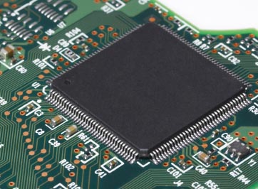
Integrated circuits (ICs) are generally the ultimate source of unintentional electromagnetic emissions from electronic devices and systems. However, ICs are too small to radiate significantly themselves. In order to radiate fields strong enough to cause an interference problem, energy must be coupled from the IC package to larger structures that act as antennas such as circuit board planes, heatsinks or cables. There are only three ways that energy can be coupled from an IC to surrounding structures:
Conducted CouplingThe figure below shows a magnetic near-field scan just above the surface of an IC package. The magnetic fields are strongest just above the lead frame where the currents are the strongest. As the figure illustrates, the strongest currents are flowing in and out of the IC through the VCC and GND pins. This is an example of simultaneous switching noise. The high-frequency currents conducted off the chip via these pins can cause significant radiated emissions by exciting the power planes or other larger structures on the printed circuit board that uses this IC. Note that while the results in the figure below involve a measurement of the near magnetic fields, the results convey information about the conducted coupling. It is not possible to quantify the magnetic field coupling based on the results of near magnetic field scans. 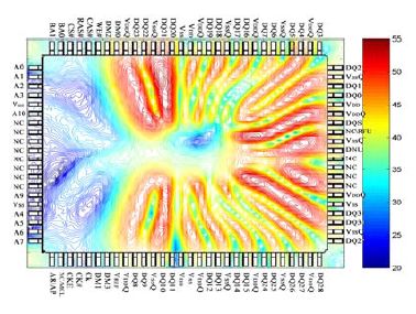
Several test procedures have been proposed to measure the conducted noise coupling from integrated circuits [1, 4 – 6]. Unfortunately, each of these measurements loads the outputs of the device-under-test with an impedance that may or may not represent the load impedance that the device will see in a real application. It isn’t possible to fully characterize an unknown source with a single voltage or current measurement. More information is required if we want to know how much conducted noise will be generated in different situations. In theory, a circuit source can be fully characterized by two measurements; an open-circuit voltage measurement and a short-circuit current measurement. In reality, at high frequencies open-circuit loads can have significant capacitance and short-circuit loads can have significant inductance. However, when these parasitic capacitances and inductances are known and controlled, it is still possible to characterize the source (at least the source parameters that will matter in real-world applications) using one high-impedance and one low-impedance measurement. These measurements results can then be used to build a Thevenin equivalent source model as shown in the figure below. Since the source voltage will depend on a variety of factors including software, the device should be measured in various situations and the worse-case parameters entered into the model. Also, since this is a one-port measurement, all possible ports (pin pairs) should be evaluated. 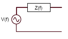
Voltages and currents can be difficult to measure directly when the load impedances are very high or very low. For this reason, it may be desirable to set the high impedance at a few hundred ohms and the low impedance at a few ohms. This will be sufficient to characterize most IC sources in the frequency ranges of interest. The Thevenin equivalent model in the figure is much simpler than ICEM and LECCS models, which serve a similar function. However, this model is sufficient for many types of worst-case emissions modeling and the complexity of the model is consistent with the number of measurements used to derive it. ELECTRIC FIELD COUPLINGThe figure below illustrates an example of electric field coupling from an IC. In this case, the “antenna” is a large heatsink being driven against the circuit board ground plane. This is an important coupling mechanism and the noise coupled from an IC/package structure through electric-field coupling is very dependent on the design of the IC and package. Unfortunately, existing field-coupling measurements for ICs [2, 5] are incapable of distinguishing between electric and magnetic field coupling. Because of this, measurement results cannot be used to represent the IC in EM coupling models. 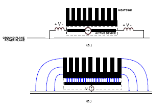
Recent research has helped to quantify how ICs couple to the structures on printed circuit boards that serve as antennas resulting in radiated emissions problems [7]. Most lines of electric flux emanating from an IC are captured by the circuit board or nearby metal objects and do not contribute significantly to radiated emissions below 1 GHz. On the other hand, electric field lines that escape the immediate environment of the IC/package structure induce common-mode currents on cables and chassis components. These common mode currents are generally responsible for unwanted radiated emissions. Recently, it was shown that hybrid TEM cell measurements are capable of quantifying the electric field coupling potential of an IC/package configuration [8]. TEM cell measurements can be used to create models that express the ability of the IC to couple to external objects. These models can replace the complex IC/package structure in full-wave system models. Thus, with a single, repeatable measurement, it is possible to capture all the relevant information about an IC/package’s ability to couple noise to external objects through an electric field. MAGNETIC FIELD COUPLING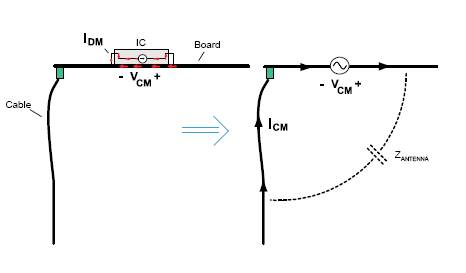
The figure on the right illustrates an example of magnetic field coupling from an IC. In this case, the “antenna” is a cable being driven against the part of the circuit board on the opposite side of the IC. Magnetic flux generated by the IC wraps around the circuit board and generates a voltage across the board capable of driving high frequency currents onto the cable resulting in radiation. The same hybrid TEM cell set-up that is used to measure electric-field coupling can be used to measure magnetic-field coupling. Generally, magnetic fields from IC/package structures cause radiated emissions problems when they wrap around other conductors (e.g. the circuit board’s ground plane) and generate a voltage across the conductor that drives common-mode currents onto cables or to other conducting objects that serve as antennas. Hybrid TEM cell measurements quantify an IC/package’s ability to couple to nearby objects in this manner. Just as an electric-field hybrid TEM cell measurement can be used to determine an “electric moment”; a magnetic-field hybrid TEM cell test can be used to determine a “magnetic moment” that can represent the IC/package in full-wave simulations [9, 10]. REFERENCES[1] IEC 61967-1 Integrated circuits - Measurement of electromagnetic emissions, 150 kHz to 1 GHz - Part 1: General conditions and definitions, International Electrotechnical Commission, Geneva, Switzerland, March 2002. [2] IEC 61967-2 Integrated circuits - Measurement of electromagnetic emissions, 150 kHz to 1 GHz - Part 2: Measurement of radiated emissions, TEM-cell and Wideband TEM-cell method, International Electrotechnical Commission, Geneva, Switzerland, Draft 47A/619/NP, October 2001. [3] IEC 61967-3 Integrated circuits - Measurement of electromagnetic emissions, 150 kHz to 1 GHz - Part 2: Measurement of radiated emissions, Surface scan method, International Electrotechnical Commission, Geneva, Switzer-land, Draft 47A/620/NP, October 2001. [4] IEC 61967-4 Integrated circuits - Measurement of electromagnetic emissions, 150 kHz to 1 GHz - Part 4: 1Ω/150Ω direct coupling method, International Electrotechnical Commission, Geneva, Switzerland, April 2002. [5] IEC 61967-5 Integrated circuits - Measurement of electromagnetic emissions, 150 kHz to 1 GHz - Part 5: Workbench Faraday cage method, International Electrotechnical Commission, Geneva, Switzerland, February 2003. [6] IEC 61967-6 Integrated circuits - Measurement of electromagnetic emissions, 150 kHz to 1 GHz - Part 5: Magnetic probe method, International Electrotechnical Commission, Geneva, Switzerland, June 2002. [7] H. Shim and T. Hubing, “Model for estimating radiated emissions from a printed circuit board with attached cables due to voltage-driven sources,” IEEE Transactions on Electromagnetic Compatibility, vol. 47, no. 4, Nov. 2005, pp. 899-907. [8] S. Deng, T. Hubing and D. Beetner, “Characterizing the electric-field coupling from IC-heatsink structures to external cables using TEM-cell measurements,” IEEE Transactions on Electromagnetic Compatibility, vol. 49, no. 4, Nov. 2007, pp. 785-791. [9] T. Hubing, S. Deng, and D. Beetner, “Using electric and magnetic ‘moments’ to characterize IC coupling to cables and enclosures,” Proceedings of EMC Compo 2007 Conference, Turin, Italy, November 2007. [10] S. Deng, T. Hubing and D. Beetner, “Using TEM cell measurements to estimate the maximum radiation from PCBs with attached cables due to magnetic field coupling,” IEEE Transactions on Electromagnetic Compatibility, vol. 50, no. 2, May 2008, pp. 419-423. |