
Printed Circuit Board Layout for EMC and Signal Integrity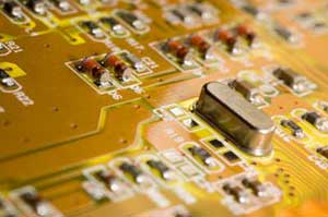
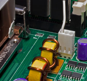
DescriptionPrinted circuit board layout is often the single most important factor affecting the electromagnetic compatibility of electronic systems. Boards that are auto-routed or laid out according to a list of “design rules” do not usually meet electromagnetic compatibility requirements on the first pass; and the products using these boards are more likely to require expensive EMC “fixes” such as ferrites on cables and shielded enclosures. Taking the time to ensure that components are properly placed and traces are optimally routed will generally result in products that meet all electromagnetic compatibility and signal integrity requirements on time and on budget. Proper layout is particularly important in mixed-signal boards (boards with both analog and digital circuits). Minor mistakes in the layout of these boards can make the difference between a reliable product and a product with severe susceptibility problems. Recognizing poor design features early in a product’s development, can save a lot of time and expense later on. This course stresses the fundamental concepts and tools that board designers must be familiar with to avoid electromagnetic compatibility and signal integrity problems. Students completing the course will be able to make good decisions regarding component selection, component placement, and trace routing. In addition, students will have the knowledge and tools necessary to design effective power distribution and grounding strategies for both digital and mixed-signal boards. 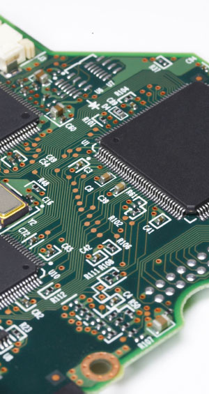
Course Outline
Course Instructor
ScheduleTo schedule an offering of this course in your city or at your company,
contact the Clemson Vehicular Electronics Laboratory at
|

![]()
Return to CVEL Home Page