Initially, the relative permittivity of the dielectric slab is set to 1.0. Thus, the configuration is a half-wavelength dipole in free space. The input file for SIFT5 is as follows,
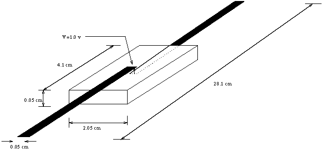
# example 3: a dipole driven by a voltage source located within the FEM region
unit 0.25 mm
boundary 0 0 0 164 82 2
celldim 0 2 2 x
celldim 2 162 16 x
celldim 162 164 2 x
celldim 0 40 10 y
celldim 40 42 1 y
celldim 42 82 10 y
celldim 0 2 1 z
dielectric 0 0 0 164 82 2 1.0 0.0
conductor -480 40 2 82 42 2 10 1 1
conductor 82 40 0 644 42 0 10 1 1
isource 82 41 0 82 41 2 533 z 1
output -480 40 2 0 42 2 y example3.out
output 164 40 0 644 42 0 y example3.out
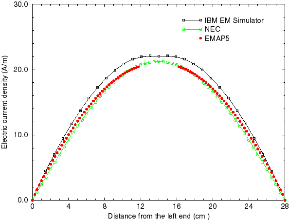
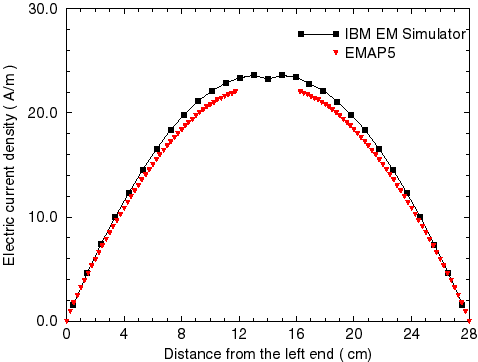
The source is modeled as a current filament that coincides with two tetrahedron edges. Near the junction and source areas, small cells are used. The FEM region is divided into 1200 tetrahedra. The boundary is divided into 2632 edges. The number of unknown edges for the final matrix equation is 1900. This problem requires 80 Megabytes memory and 20 hours to run on a Sun Ultra workstation. The current distribution on the traces obtained using EMAP5 is plotted in Figure 14. For comparison, the results obtained using the Numerical Electromagnetics Code (NEC) and the IBM EM Simulator are also plotted. Figure 15 shows the results obtained by EMAP5 and the IBM EM Simulator when the dielectric constant is set to 10.0. In both cases, the results obtained using the different methods are similar.