A. Determining the Characteristic Impedance of a Microstrip Geometry
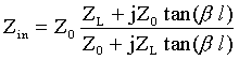
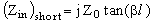
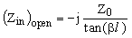
This example simulates a microstrip line on a printed circuit board. The geometry of the structure is shown in Figure 1. The board is made of a dielectric with e r=4.0. The trace is excited by a 1V s ource at one end, and is terminated by a resistor at the other end. To determine the characteristic impedance Z0 of the transmission line, we need to determine the input impedance when the load side is shorted or open, respectively. The input impedance Zin of a transmission line is given by,
where (xf, yf) specifies its position, I
denotes the electric current magnitude, and d
(x) is the Dirac delta function. Jint is the impressed current
source. After the E fields along the source edges are obtained, the voltage
drop along the current filament can be calculated. Thus, the input impedance
Zin can be obtained.
The input file for SIFT5 is as follows(Source frequency is 300 MHZ,
the load side is shorted):
# example 5: Use EMAP5 to determine the input impedance of
# a microstrip antenna when it is shorted at the load side.
# the unit is set to be one millimeter
unit 1 mm
# the dimension of the board is 60 mm * 54 mm * 2 mm
boundary 0 0 0 60 54 2
# use uniform mesh along the X axis
celldim 0 60 5 x
# use uniform mesh along the Y axis, the fields near the traces
# changes dramatically, thus use fine mesh near the trace region.
celldim 0 14 7 y
celldim 14 18 4 y
celldim 18 36 2 y
celldim 36 40 4 y
celldim 40 54 7 y
# use uniform mesh along the X axis
celldim 0 2 2 z
# the permittivity of the substrate is 4.0.
dielectric 0 0 0 60 54 2 4.0 0.0
# the active trace
conductor 20 20 2 40 24 2 5 10 10
# the load side is shorted
conductor 40 20 0 40 24 2 5 5 5
# the ground plane
conductor 0 0 0 60 54 0 10 10 10
# the source
einter 20 22 0 20 22 2 300 z 1.0 0
# print the E field along the source edge
output 20 22 0 20 22 2 z E5.out
When the load side is open, we need to delete the following lines:
# the load side is shorted
conductor 40 20 0 40 24 2 5 5 5
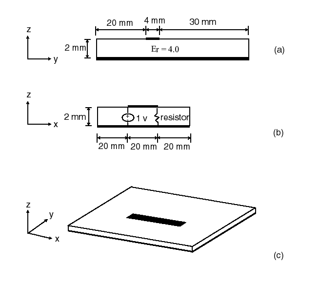
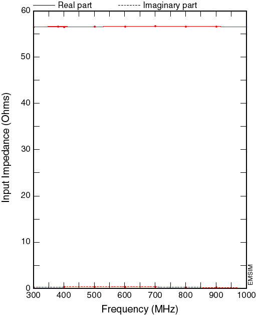
Table 1 shows inductance and capacitance obtained by EMAP5 when the load side is shorted or open, respectively. The characteristic impedance Z0 of the trace then can be determined. Three frequencies have been investigated. At each fre quency, the calculated value of Z0 is 56.4 W. We can put a 56.4 W resistor at the load side to terminate the transmission line. Theoretically, there should be no reflection if Z0 is 56.4 W . Figure 2 shows the numerical results obtained by EMSIM when the trace is terminated with a 56.4 W resistor. It is evident that the transmission line is almost perfectly matched.
|
|
|
|
|
|
|
|
|
|
|
|
|
|
|
|
|
|
|
|
B. Determining the Input Impedance of a Microstrip
Line with a Resistive Load.
In this example, the configuration is the same as shown in Figure 1.
Now however, the load is a 50 W resistor. A
load ZL can be modeled as an element with finite conductivity
given by s =l/(ZLS), where
l is its length, and S is the cross section. If the load is treated
as a lumped element, its contribution to the finite element matrix is as
follows [8]:
![]()
where (xL, yL) is the position of the load impedance.
Only edges coinciding with the load are affected by the load.
The following line should be added to the input file for SIFT5:
resistor 40 22 0 40 22 2 50
The above line defines an edge coincidingd with a 50 ohm resistor. If one wants to model the resistor as two edges, each edge should have a value of 25 ohms.
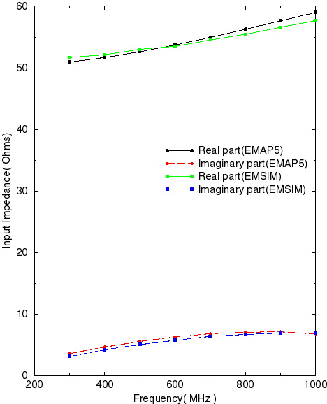
Figure 3 shows the impedance obtained by EMAP5 and compares them with results obtained by EMSIM. Since the characteristic impedance of the microstrip line is about 56.4 W, the 50 W load does not match the microstrip line perfectly. As shown in Figure 3, the input impedance is not exactly 50 W due to the mismatch. The EMAP5 results agree very well with the EMSIM results for this example.