PCB Power Bus without Cable
 |
|
This canonical geometry is basically a pair of perfectly conducting planes with a
slightly lossy dielectric material between them. It emulates a printed circuit board
power bus (or microstrip patch antenna), which can be a significant source of radiated
emissions at frequencies corresponding to resonances of the cavity formed between the planes.
Modeling Notes:
θ=0° is the angle directly above the center of the
top plate. The frequency range 5 MHz - 2 GHz includes the following cavity
resonances: TM10@566MHz,
TM01@707MHz, TM11@906MHz, TM20@1.13GHz, TM21@1.33GHz, TM02@1.41GHz, TM12@1.52GHz,
TM30@1.7GHz, TM22@1.81GHz, TM31@1.84GHz. Due to the source's location in the center
of the shorter edge, we do not excite TMx1 resonances.
|
|
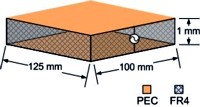
Geometry |
PCB size: 125 mm × 100 mm × 1 mm
|
Material |
Top layer: PEC
Middle layer: FR4, εr = 4.5, dielectric loss tangent = 0.015
Bottom layer: PEC
|
Excitation |
Voltage Source (1 V, 50 ohms ) or Current Source (0.02 A, 50 ohms )
Location: middle of the short edge |
Output |
- Plot of the input impedance (5 MHz - 2 GHz )
- Plot of electric field ( 5 MHz - 2 GHz, 3 m, θ=0°, φ=0° )
- Plot of electric field ( 5 MHz - 2 GHz, 3 m, θ=90°, φ=90° )
|
|