 |
|
Modeling a printed circuit board alone in free space can be challenging, but printed circuit
boards usually have cables attached to them and are nearly always tested above a conducting
ground plane. Adding a cable and a ground plane to the geometry of the previous problem
significantly complicates the modeling process. Several codes are not capable of modeling this
geometry and nearly all of the codes have difficulty with it. This problem incorporates many
basic features typically found in practical problems of interest to EMC engineers.
Modeling Notes:
The wire has a circular cross section with a 2-mm radius. However, equivalent results
can be obtained by modeling the wire with a flat ribbon that has an 8-mm width. The radiated field plots exhibit peaks corresponding to board cavity resonances (above
500 MHz) as well as lower-frequency peaks corresponding to resonances associated with the cable-board
structure.
|
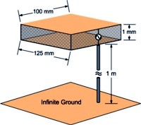
PCB & Cable Dimensions |
| PCB size | 125 mm × 100 mm × 1 mm |
| Cable length | 1 m |
| Cable radius | 2 mm |
|
PCB & Cable
Materials |
All conductors (plates and cable) are perfectly conducting.
Board Dielectric: FR4, εr = 4.5, dielectric loss tangent = 0.015
|
Ground Plane |
Location: 1 m below the PCB board
Size: infinite
Material: PEC
|
Excitation |
Voltage Source (1 V, 50 ohms ) or Current Source (0.02 A, 50 ohms )
Location: middle of the short edge, between the PCB planes |
Outputs |
- Plot of electric field ( 5 MHz - 2 GHz, 10 m, θ=0°, φ=0° )
- Plot of electric field ( 5 MHz - 2 GHz, 10 m, θ=90°, φ=0° )
- Plot of electric field ( 5 MHz - 2 GHz, 10 m, θ=90°, φ=90° )
- Plot of electric field ( 5 MHz - 2 GHz, 10 m, θ=90°, φ=180° )
|
|