Modeling Powerbus and Cable with EMAP
Geometry and setup |
Double-sided PCB:
- Size: 125 mm × 100 mm × 1 mm
- Top and bottom metal: PEC
- Dielectric: FR4, εr = 4.5, dielectric loss tangent = 0.015
Cable:
- Length: 1000 mm
- radius: 2 mm
- Material: PEC
Excitation: Current source (0.02 A, 50 ohms)
Mesh Setup:
- Dielectric mesh size: 1 mm × 8 mm
- PEC mesh size: 8 mm × 8 mm
Frequency Setup: 10 MHz - 2 GHz, Step Size = 10 MHz
|
Simulation result |
Simulation Time: 14 hrs 20 mins
Number of triangles: 1052
Number of tedrahedra: 2322
Number of edges: 3684
|
Decisions the user must make that affect the accuracy of the result |
- Thickness of dielectric: 1 mm, thicker gives different E
- Number of triangles and tetrahedra: more better (dependent on RAM)
- Aspect ratio of triangles and tetrahedra: less than 5
|
Comments |
Please refer to the PowerBus model for comments that are common with the PowerBus with cable model.
- How is the cable modeled?
A flat PEC ribbon is used to model the cable. The width of the ribbon is
4 times the radius of the cable.
One end of the ribbon is attached to
the infinite conducting ground at z=0. The other end is attached to the metal part of the powerbus.
The edges at this end should overlap with the edges of the metal edges they join to. The joint can
be placed at the boundary edge of the metal. Thus a junction edge is formed because at this/these
edges, three triangles share one edge. The joint can also be place inside the metal surface.
|
|
|
Screen shots
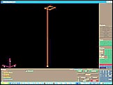
Fig. 1. Simulation model
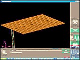
Fig. 2. Simulation meshes
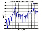
Fig. 3. Electric field at 10 m, θ=0°, φ=0°
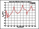
Fig. 4. Electric field at 10 m, θ=90°, φ=0°
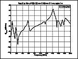
Fig. 5. Electric field at 10 m, θ=90°, φ=90°
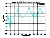
Fig. 6. Electric field at 10 m, θ=90°, φ=180°
|
|
)
)
)
)
)
)