Modeling a Powerbus with HFSS (version 11.1.3)
|
Geometry and setup |
Double-sided PCB:
- Size: 125 mm × 100 mm × 1 mm
- Top and bottom metal: PEC
- Dielectric: FR4, εr = 4.5,
dielectric loss tangent = 0.015
Solution type:
Driven terminal
Excitation: Voltage source (1 V, 50 ohms)
Boundary: Radiation
Analysis Setup:
- Solution Frequency: 1.15 GHz
- Maximum Number of Passes: 50
- Maximum ΔS: 0.01
- Do Lambda Refinement: 0.4
- Maximum Refinement Passes: 20%
Sweep:
- Sweep type: Discrete
- Frequency Setup: 5 MHz - 2 GHz, Step Size = 5
MHz
 hfss_powerbus.zip hfss_powerbus.zip
|
|
Simulation result |
Simulation Time: 44 mins 50 secs
Number of passes completed: 7
Number of tetrahedra: 3776
|
|
Decisions the user must make that affect the
accuracy of the result |
- Solution type: driven terminal
- Location of absorbing boundary: cylinder, radius=150 mm, height=300 mm
- Maximum ΔS: default = 0.02, this model = 0.01
- Do lambda refinement: default = 0.333, this model =0.4
- Maximum refinement passes: default=30%, this model=20%
|
|
Comments |
- How did we select the solution
type?
Two kinds of solution types are available in HFSS, Driven
Modal and Driven Terminal. We used the Driven Modal solution type
to calculate the input impedance and the Driven Terminal
solution type to calculate the far-zone
radiation.
- How did we select the excitation
type?
In HFSS, impedance matrix parameters are computed from the
S-parameters and port impedances. Since lumped ports compute
S-parameters directly at the port, it is more efficient to use a
lumped port when you want HFSS to calculate the input impedance and assign a voltage source when you want to specify the voltage and
direction of the electric field on a surface. In this model, the
power bus is driven by a 50-ohm source. To simulate the source, an ideal voltage source
was assigned to a rectangle from the edge of the upper layer to
the RLC boundary. The RCL boundary was modeled as a 50-ohm resistor
in series with the ideal voltage source.
| |
Screen shots
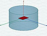
Fig. 1. Simulation model
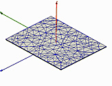
Fig. 2. Simulation meshes
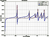
Fig. 3. Input impedance
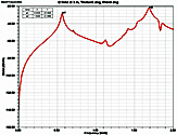
Fig. 4. Electric field at 3 m,
θ=0°, φ=0°
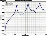
Fig. 5. Electric field at 3 m,
θ=90°, φ=0°
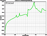
Fig. 6. Electric field at 3 m,
θ=90°,
φ=90° | |
)
)
)
)
)
)