Modeling the Inductance of an SMT Capacitor with Q3D
Geometry and setup |
Capacitor dimensions:
- Pad size: 0.5 mm × 0.5 mm × 0.017 mm
- Cathode/Anode: 0.5 mm × 0.1 mm × 0.5 mm
- Plate: 0.5 mm × 0.7 mm × 0.05 mm
- Dielectric: 1.5 mm × 1.8 mm × 0.1 mm
- Gap b/w two plates: 0.4 mm
- Capacitor size: 1005
PCB dimensions:
- Dielectric thickness: 0.1 mm
- Pad size: 0.5 mm × 0.5 mm
- Copper thickness: 0.017 mm
- Via: 0.1 mm (outer radius), 0.08 mm (inner radius)
- Space b/w package vias: 0.8 mm
- Distance b/w package via and cap via: 2.5 mm
Dielectric: εr = 4.4
Solver Setup:
Solver residual: 1e-005
Solution frequency: 1 GHz
Conduction Adaptive Solution:
- Maximum number of passes: 10
- Minimum number of passes: 1
- Minimum converged passes: 1
- Percent error: 1%
- Percent refinement per pass: 30%
Multipole Adaptive Solution:
- Maximum number of passes: 10
- Minimum number of passes: 1
- Minimum converged passes: 1
- Percent error: 1%
- Percent refinement per pass: 30%
 q3d_smtind.zip
 |
Simulation result |
Self loop inductance: 0.59043 nH
|
Decisions the user must make that affect the accuracy of the result |
- PCB stack-up dimension & capacitor structure that form a loop for the extraction of a effective inductance
- Solver residual : 1e-005
- Solving frequency : 1GHz
|
Comments |
- What is the difference between AC and DC inductance?
At DC, currents flow relatively uniformly throughout a conductor. At high frequencies, the skin effect
forces currents to flow near the surface of conductors. This difference in the current distributions
translates to a difference in the inductance. At frequencies above a few hundred MHz, the currents in metal
conductors are generally confined to the surface and AC calculations are most appropriate. At lower frequencies,
or in poorer conductors, the skin depth should be calculated and compared to the thickness of the conductors.
If the conductors are not thick relative to a skin depth, then the DC inductance is probably a more appropriate
choice.
- Where should the source and sink be located?
Inductance is a property of current loops. The source and sink should be located near each other and the current
should be forced to flow in a well-defined loop. Q3D allows the source and sink to be placed at points distant
from each other and does not care if the current flows in a loop. In situations where there is not a well defined
loop, the output from Q3D is a partial inductance (actually a matrix of partial-self and partial-mutual inductances)
that has relatively little meaning in practical applications.
|
|
Screen shots
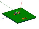
Fig. 1. Simulation model
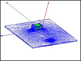
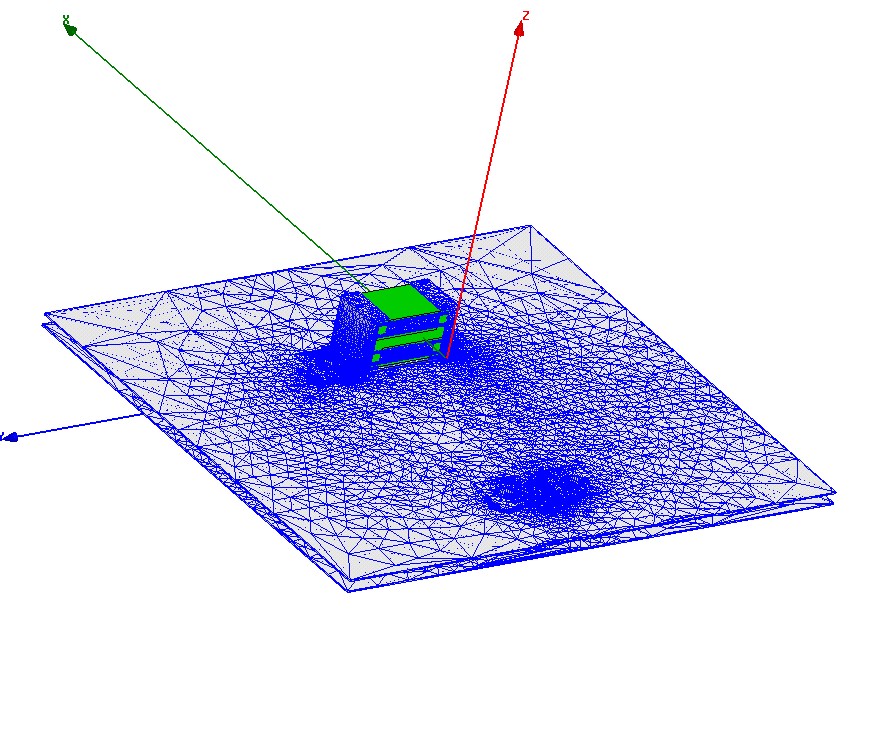
Fig. 2. Simulation meshes
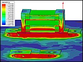
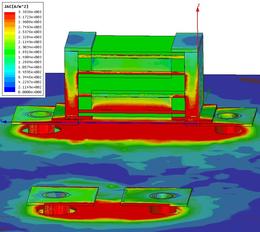
Fig. 3. AC current distribution
|
|