Modeling a Powerbus with FEKO
|
Geometry and setup |
Double-sided PCB:
- Size: 125 mm × 100 mm × 1 mm
- Top and bottom metal: PEC
- Dielectric: FR4, εr = 4.5,
dielectric loss tangent = 0.015
Mesh:
- Global mesh size: Edge length=6 mm, Segment
length=0.2 mm, wire radius=0.01 mm
- Disable volume meshing
- Small features: default
- Advanced: Enable mesh smoothing
Solution
- Settings: Double precision
- Frequency: continuous (interpolated) range:5
MHz - 2 GHz, maximum number of samples=200
- Excitations: Voltage source (1 V, 50 ohms)
- Calculation: Far field, θ=0° -
90°, φ=0° -
90°
 feko_powerbus.zip feko_powerbus.zip
|
|
Simulation result |
Number of metallic triangles : 2187
Number of dielectric triangles: 205
Number of metallic edges (MoM): 6314
Number of basis function for MoM: 6929
Run time: 2
hours
|
|
Decisions the user must make that affect the
accuracy of the result |
- Uncheck the 'Enable volume meshing' option. For the power bus
problem, the MOM analysis will be accurate.
|
|
Comments |
- How can we model the powerbus model?
Actually, there
are two methods to create this double-sided PCB.
1) Create
the dielectric substrate by defining a rectangular block and
assign a dielectric medium to it. Then, assign the PEC attribute
to its top and bottom faces.
2) Create the substrate block and
assign a dielectric medium to it. Draw two polygons (rectangles).
One touches the top face of the dielectric solid and another
touches the bottom face. They are perfect conductors by default.
The first method is the most straightforward way of doing
this. The problem with the second method is that when you make a
union of a dielectric block and a PEC surface that coincides with
a face of the dielectric, the face may be "absorbed" into the
dielectric and lose its PEC property. Thus you would have to
reassign the PEC property to the face. Therefore it is recommended
to use the first method.
- Can a feed be located at the edge of the plane surface?
In FEKO, voltage sources are not applied directly to the
model geometry or mesh. A port must be defined on the geometry or
mesh before adding the required source or load. In this example,
the voltage source is located at one edge of the PCB. However, in
FEKO, the edge for a port is not allowed to be on the surface of
the dielectric.
More
information... | |
|
Screen shots
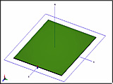
Fig. 1. Simulation model
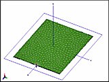
Fig. 2. Simulation meshes
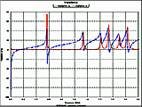
Fig. 3. Input impedance
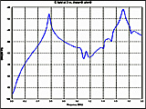
Fig. 4. Electric field at 3 m,
θ=0°, φ=0°
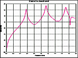
Fig. 5. Electric field at 3 m,
θ=90°, φ=0°
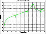
Fig. 6. Electric field at 3 m,
θ=90°,
φ=90° | |
)
)
)
)
)
)