![]()

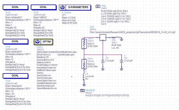
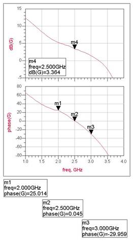
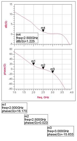
Use of Agilent Advanced Design System Wide-Locking Range Oscillator Design using ADS Optimization Routine: First, the oscillator was designed using lumped components. The transistor, a NE38018 from NEC, is represented by its 2-port S parameters. The optimization routine used 4 "Goals": one for magnitude of loop gain, and three for minimizing the slope of the loop gain phase. The inductor, capacitor, and load impedance were all optimization variables.
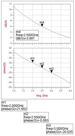
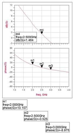
The first graph shows the results before optimization, and the second graph, after optimization. Initially, the loop gain was 4dBm with a phase slope of 40°/GHz; after optimization, 1.46dBm with a phase slope of 22°/GHz. This corresponds to an improvement in locking range from about 65MHz to 135MHz at -25dBm injection power.
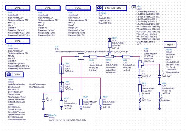
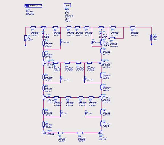
The circuit was then analyzed using microstrip transmission lines in place of the lumped components. The same four "Goals" were used, but here the transmission line lengths and width were the optimization variables.
Again, notice the results before optimization and then after optimization. Initially, the loop gain was 3.36dBm with a phase slope of 55°/GHz; after optimization the loop gain was 1.23dBm with a phase slope of 32°/GHz. This corresponds to an improvement in locking range from 60MHz to 85MHz at -25dBm.
Measured results have not yet been obtained for these oscillators. Previously, with this same procedure, it was shown that progressively decreasing the phase slope, through the optimization routine in ADS, the measured locking range of the oscillators did improve (taken from the Ph.D. dissertation of Xing Wang).
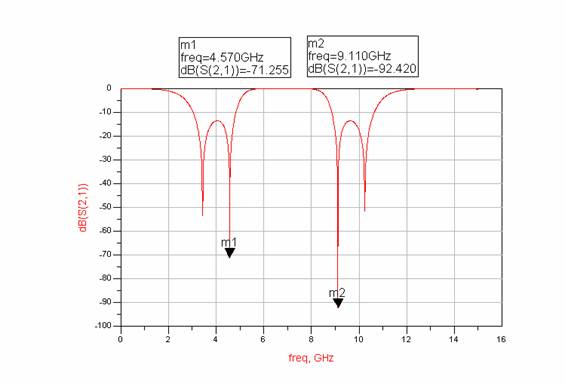
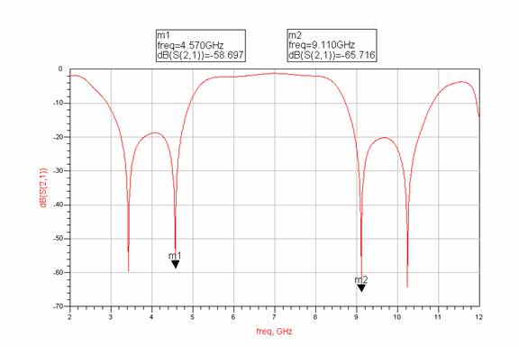
Microwave Transversal Band Pass Filter Design using ADS: The
The first cycle of the filter is alone utilized. The filter has a stop band attenuation of around -13 dB. The desired filter was designed for a pass band attenuation of 2dB and a stop band attenuation of 20dB.
|
|
Center for Research in Wireless Communications, 301 Fluor Daniel Engineering
Innovation Building College of Engineering and Sciences -- Electrical and Computing Engineering -- Web Accessibility
Copyright © 2003, Clemson University. All rights reserved. Clemson University, Clemson, South Carolina 29634 Area Code: 864, Information: 656-3311 |